Graduate School of Science, Technology and Innovation, Kobe University
General description
Throughout our continuous research and education on the advanced hardware systems at Kobe university, students in the graduate school will gain knowledge of ‘security and safety’ along with ‘analogue and digital’ and experience the practical merge of them in scientific research works and technical developments. Our academic backgrounds involve the design and evaluation of very large-scale integration (VLSI) systems, the electromagnetic compatibility (EMC), the authenticity and security of hardware devices. Semiconductor solid-state circuits and integrated circuit (IC) chips are always located in the heart of developments. Our alumni contribute to our sustainable society through the innovation of advanced and ubiquitous information and communication technologies. So far, we have more than 80 graduates, including 25 doctoral degree recipients. The laboratory logo of ‘Secafy’ stands for our research activities on hardware security and safety.
research topics
01Hardware security
The design and development of highly functional cryptographic hardware for securing confidentiality, integrity, availability and authenticity of information data.
The demands are continuously growing on information and communication technology (ICT) that can safely and securely manipulate information data with high confidentiality, in the era of internet of things (IoT). We are challenging exploration toward a comprehensive body of novel technologies of hardware for security. Research topics widely cover the cryptographic engines with high functionality and efficiency, the authenticity of device itself from designs to supply chains, the resiliency against attacks of snooping mainly through side channels, and so forth.
02Hardware Safety
The principles of highly reliable electronics hardware, assuring operational safety under harsh environment with diversified disturbances.
Hardware systems are generally placed in a variety of physical locations, and as a result suffer from the surrounding environment (specially by electromagnetic (EM) waves that are unseen by humans). Wireless communication transmitting and receiving large amount of data uses a very subtle EM power. The vehicle to vehicle, as well as to roadside communication units and supporting electronics, and advanced medical and healthcare appliances and supporting electronics, are operating under an dynamically changing environment where hardware-level safety is strongly demanded for robustness, reliability and security. We are studying hardware safety with particular emphasis on the design principles of electronics with high resiliency for electromagnetic interference (EMI) and electromagnetic susceptibility (EMS), mostly at semiconductor IC chip level.
03quantum computer
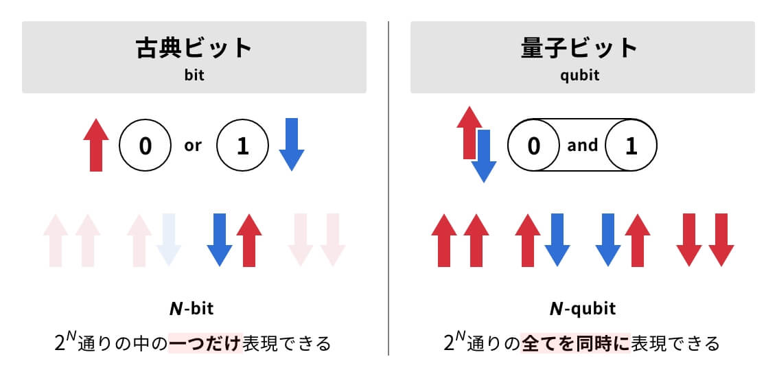
量子コンピュータは、量子力学の性質を応用した次世代コンピュータです。量子重ね合わせ(Superposition)や、量子もつれ(Entanglement)といった量子力学の現象を有効活用し、現在のコンピュータでは解けないような大規模な演算を瞬時に解くことができると言われています。そのため、量子コンピュータは、暗号や化学、金融、AIといった幅広い分野で応用されることが期待されています。
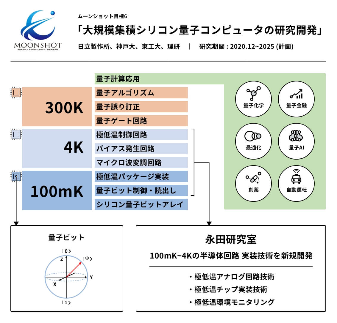
現在、GoogleやIBMを中心に世界中で量子コンピュータ研究の熾烈な競争が繰り広げられています。日本でも、内閣府からムーンショット型研究開発事業がスタートし、その目標の一つとして「2050年までに、経済・産業・安全保障を飛躍的に発展させる誤り耐性型汎用量子コンピュータを実現」が掲げられました。永田研究室は、(株)日立製作所、東京工業大学、理化学研究所と共にこのムーンショット型研究開発事業の一つである「大規模集積シリコン量子コンピュータの研究開発」に参画しています。
Role and theme of our laboratory
永田研究室の役割は、シリコン量子コンピュータの核であるシリコン量子ビットを正確に制御するための、回路・実装技術の研究です。特に、シリコン量子ビットは絶対零度に限りなく近い温度(約100mK)に保つ必要があるため、極低温(100mK~4K)における量子ビット制御回路や、量子ビットチップの実装技術が求められます。しかし、極低温での回路の電気特性や熱流特性などは未知の要素が多く、既存技術を流用することができません。そこで、永田研究室では、「極低温アナログ回路」「極低温チップ実装」「極低温環境モニタリング」のテーマを掲げ、シリコン量子コンピュータの実現に貢献します。
また、永田研究室では、量子コンピュータのハードウェア研究だけでなく、量子誤り訂正アルゴリズムなどの量子ソフトウェアの研究も積極的に行っています。ハードウェアだけで実現することが困難な問題を量子アルゴリズムでカバーするなど、ハード・ソフト両面で量子コンピュータ開発に取り組んでいます。
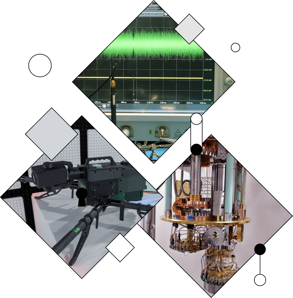
Cryogenic analog circuit
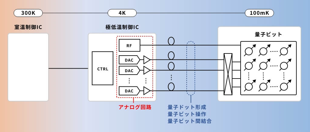
量子コンピュータは、量子ビットの操作・読出し・初期化といった制御を行うことで量子演算を実行します。これらの制御を実現するためには、バイアス電圧やマイクロ波を発生させる信号生成器や、量子ビットの僅かな変化を読み取るセンサーが必要です。これらは全てアナログ回路で構成されます。また、これらの回路は量子ビット近傍に配置するため、極低温で動作しなければなりません。永田研究室では、極低温アナログ回路の研究を行っており、アナログ回路の設計、チップ試作、極低温評価を一貫して行うことで、シリコン量子ビットの高精度制御を実現する極低温アナログ回路の研究を行っています。
Cryogenic chip mounting
シリコン量子ビットチップは、希釈冷凍機という冷却装置の最深部にあるチャンバーに配置されます。このチャンバー内は、スペースが限られているだけでなく、チップの発熱に対しても厳しい制約が設けられています。永田研究室では、チップを小面積・低損失でパッケージングする技術や、チップが発する熱を効率よく排熱する機構を研究しています。具体的には、極低温における信号品質の解析や熱流シミュレーション、パッケージング試作と極低温評価による検証などを行っています。
Cryogenic environmental monitoring
量子ビットは、ノイズに弱いという性質を持っています。ノイズには、熱の上昇や電磁場の変動、制御信号の誤差などが含まれます。これらのノイズが存在すると、量子ビットのフィデリティが劣化し、量子演算誤差が生じます。永田研究室では、量子ビット近傍において、これらの環境ノイズをモニタリングする手法を提案しています。得られたノイズ情報は制御回路にフィードバックすることで、演算精度の向上を目指しています。具体的な取り組みとして、極低温で動作する超低電力センサー回路等の開発を行っています。
Quantum algorithm
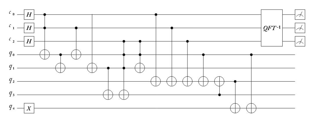
量子コンピュータのハードウェアはまだまだ開発途上であり、しばらくは様々な制約のもとでソフトウェアを構築する必要があります。ここでの制約とは、量子ビットの数と量子ビットのエラー率です。どちらも十分とは言えない現状において、ある程度「使える」アプリケーションを開発するためには、ハードウェアの改善に加え、量子誤り訂正等の量子アルゴリズムを同時に研究することが重要です。永田研究室では、IBM QやAmazon Braketを活用し、実際に量子コンピュータ上で動かすソフトウェアの研究にも取り組んでいます。
